Altium PCB Rules for JLCPCB
2026-09-20
Table of Contents
- Contents
- Part 1: Project setup
- 1.1 Turn off automatic class generation
- 1.2 Change the units to millimeters
- Part 2: Design rules
- 2.1 Clearance
- 2.2 UnRoutedNet
- 2.3 Trace width
- 2.4 RoutingVias
- 2.5 PolygonConnect
- 2.6 SolderMaskExpansion
- 2.7 MinimumSolderMaskSliver
- 2.8 Save the rules
- Part 3: Layer stackup
- 3.1 What is a stackup?
- 3.2 Why does the stackup matter?
- 3.3 Why we picked JLC04161H-7628
- 3.4 When to use a different stackup
- 3.5 Set up the stackup in Altium
- Part 4: Impedance and trace widths
- 4.1 Ways to calculate impedance
- 4.2 Use Altium's impedance calculator
- Quick cheat sheet
This guide shows you how to set up Altium Designer so your board follows JLCPCB's rules. We're building a 4-layer board with JLCPCB's standard stackup, JLC04161H-7628.
What we'll do:
- Change a couple of project settings and switch to mm (Part 1)
- Set up the design rules (Part 2)
- Set up the layer stackup (Part 3)
- Calculate trace widths for impedance (Part 4)
Why bother with rules? If your design goes past what JLCPCB can make, your board can come out with problems (or they'll ask you to fix the files). With these rules set up, Altium warns you with DRC errors while you design, so you don't find out after you've paid for the boards.
Contents
- Part 1: Project setup
- Part 2: Design rules
- Part 3: Layer stackup
- Part 4: Impedance and trace widths
- Quick cheat sheet
Part 1: Project setup
Two quick settings to change before we touch any rules.
1.1 Turn off automatic class generation
- In the main menu, go to Project > Project Options...
- Click the Class Generation tab at the top of the window.
- Turn off the automatic options for component classes and net classes.
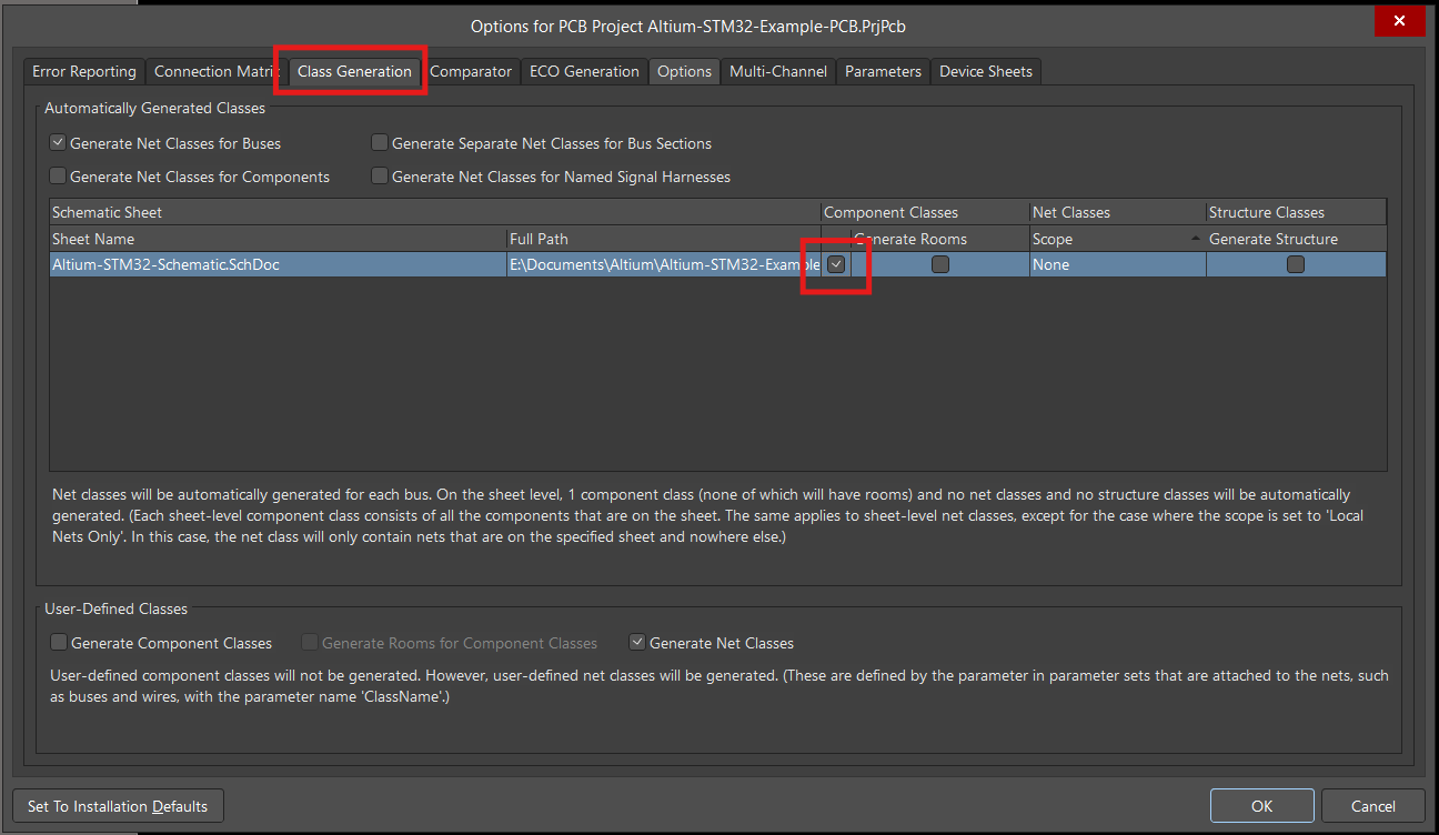
Why do this? By default, Altium creates extra component classes and layout rooms on its own. On a normal board you don't need them, and they just make the design messy. Only turn this back on if you're working on a multi-channel design or a circuit that repeats many times, where you really want those classes.
1.2 Change the units to millimeters
- Make sure nothing is selected in the PCB editor.
- Open the Panels menu in the bottom-right corner and choose Properties.
- Scroll down to the Other section.
- Under Units, pick mm.
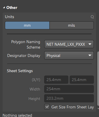
Why do this? Every number in this guide is in mm, so working in mm means you can type the values straight in without converting.
Part 2: Design rules
Now we'll tell Altium what JLCPCB can and can't manufacture. Open the rules window with Design > Rules...
The values come from JLCPCB's capabilities page: https://jlcpcb.com/capabilities/pcb-capabilities. Most of our numbers are a bit safer than JLCPCB's absolute minimum, so you get some room for error.
2.1 Clearance
What it does: Clearance is the smallest gap allowed between two things that are on different nets. If two things get closer than this, Altium shows a DRC error.
Go to Electrical > Clearance and fill in the matrix with these values (all in mm):
The table is mirrored, so you only fill in half of it. Track-to-SMD-pad is the same rule as SMD-pad-to-track.
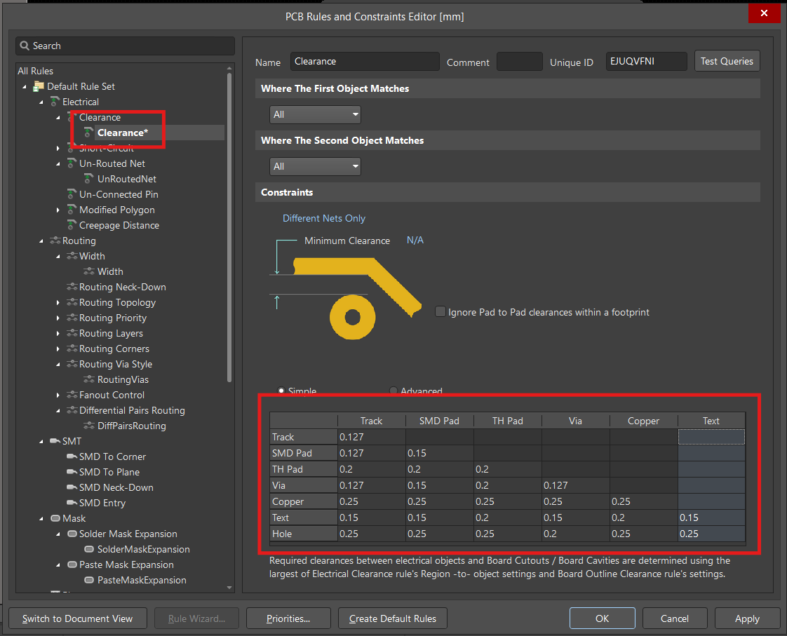
Why these numbers?
- Track / SMD pad / Via at 0.127 mm (5 mil): This is a comfortable gap for JLCPCB's normal process. Their 4-layer boards can go smaller than this, so you have some margin.
- SMD pad to SMD pad at 0.15 mm: Pads on small chips sit close together, so we give them a little extra room to avoid solder bridges.
- TH pad at 0.2 mm: Through-hole pads have drilled holes, and drilling is less precise than etching, so we keep more distance.
- Copper (polygons) at 0.25 mm: We keep copper pours further from everything so small manufacturing errors don't cause shorts.
- Text at 0.15 / 0.2 mm: This only matters for text that's on a copper layer. It keeps the text clear of other copper so it stays readable.
- Hole at 0.25 mm: This keeps copper away from unplated holes and cutouts, so the drill or router doesn't cut into it.
2.2 UnRoutedNet
What it does: Makes Altium show an error when a connection isn't finished.
Go to Electrical > Un-Routed Net > UnRoutedNet and make sure Check for incomplete connections is turned on.
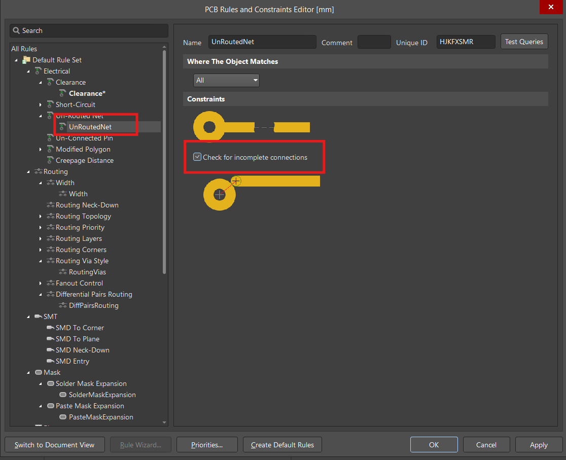
Why do this? It's easy to forget one wire on a busy board, and a board with a missing connection can be useless. This rule catches it before you order.
2.3 Trace width
What it does: Sets how thin and how wide your traces are allowed to be.
Go to Routing > Width > Width and set:
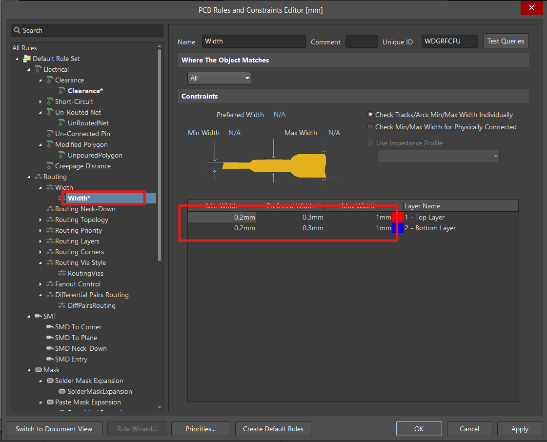
Why these numbers?
- Minimum 0.2 mm: JLCPCB can make thinner traces than this, but thicker ones are more reliable (they break or short less often).
- Preferred 0.3 mm: This is the width Altium uses when you start routing.
- Maximum 1 mm: Anything wider than this gets flagged.
Tip: This is the general rule for the whole board. Some nets need something different, like wide power traces or 90 Ω USB pairs (see Part 4). For those, make a separate rule with a higher priority, otherwise Altium will use this general one.
2.4 RoutingVias
What it does: Sets the size of the vias you're allowed to use.
Go to Routing > Routing Via Style > RoutingVias and set:
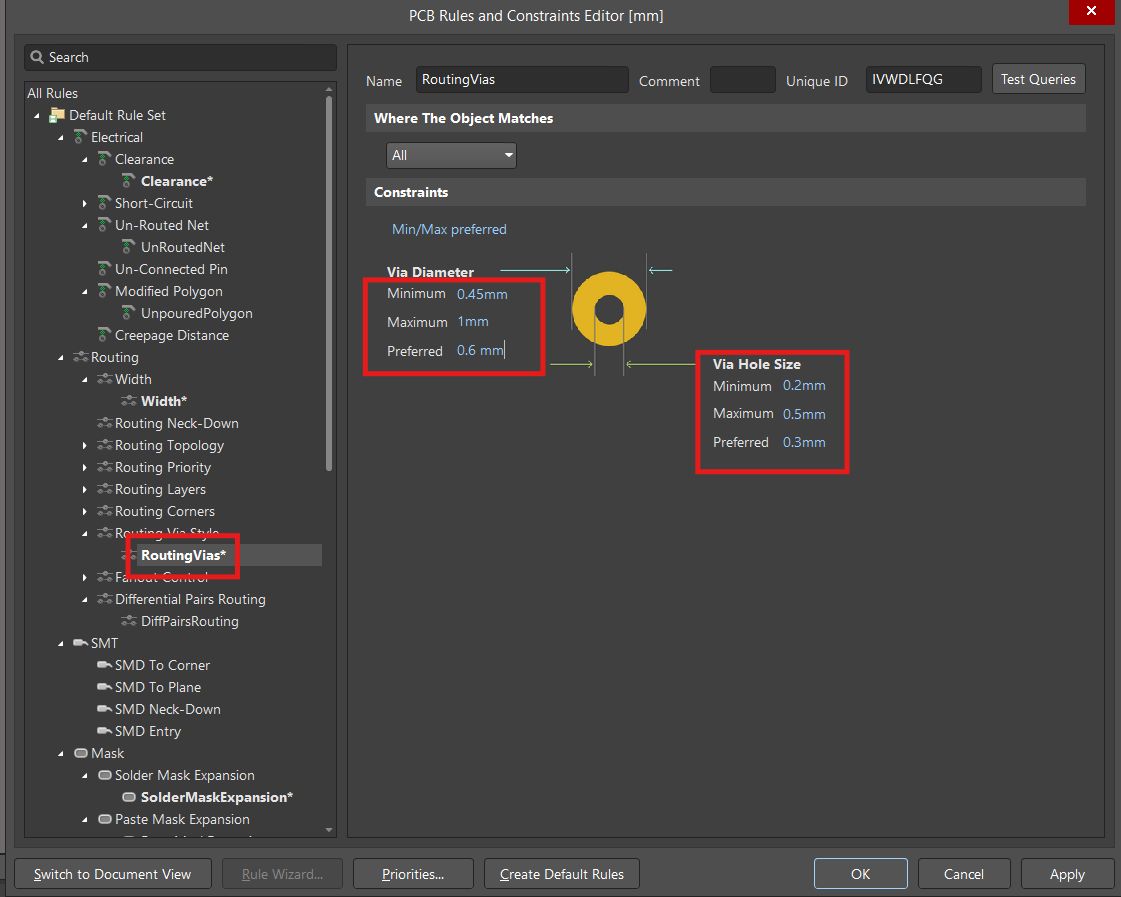
Why these numbers? The copper ring around the hole is called the annular ring, and it's half the difference between the diameter and the hole size:
- Preferred via: (0.6 − 0.3) / 2 = 0.15 mm of copper around the hole.
- Smallest via: (0.45 − 0.2) / 2 = 0.125 mm of copper around the hole.
The ring has to be big enough to survive drilling, because drills are never perfectly centered. The minimum values (0.2 mm hole, 0.45 mm diameter) are about the smallest vias JLCPCB makes on multilayer boards, and the preferred values give you a safe, easy default.
2.5 PolygonConnect
What it does: Decides how pads connect to a copper pour (polygon).
Go to Plane > Polygon Connect Style > PolygonConnect and pick the connect style you want. In this guide we use Direct Connect.
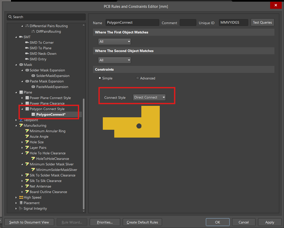
Why? It depends on your project:
- Direct Connect: The pad merges fully into the pour. This gives the best electrical and heat connection, but pads can be harder to solder because the pour pulls heat away.
- Relief / thermal relief: The pad connects through thin spokes. It's easier to solder, but the connection isn't as strong.
2.6 SolderMaskExpansion
What it does: The solder mask has an opening over each pad. This rule makes the opening a little bigger than the pad.
Go to Mask > Solder Mask Expansion > SolderMaskExpansion and set the expansion to 0.05 mm.
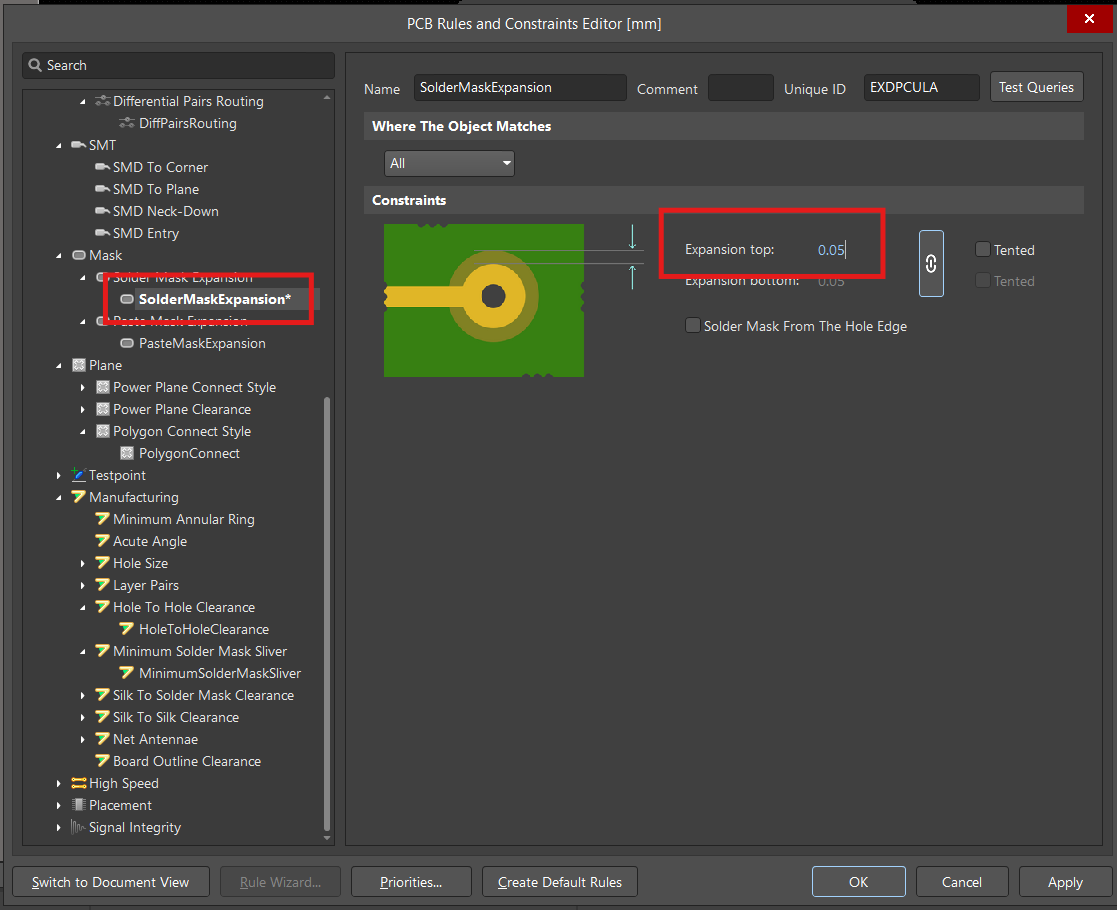
Why? The mask is never lined up perfectly with the copper. With a small extra gap (0.05 mm, about 2 mil), a tiny shift won't cover part of your pad.
2.7 MinimumSolderMaskSliver
What it does: A "sliver" is a thin strip of solder mask left between two neighboring openings (for example, between the pads of a fine-pitch chip). Really thin slivers can peel off, so this rule flags them.
Go to Manufacturing > Minimum Solder Mask Sliver > MinimumSolderMaskSliver and set it to 0.1 mm.
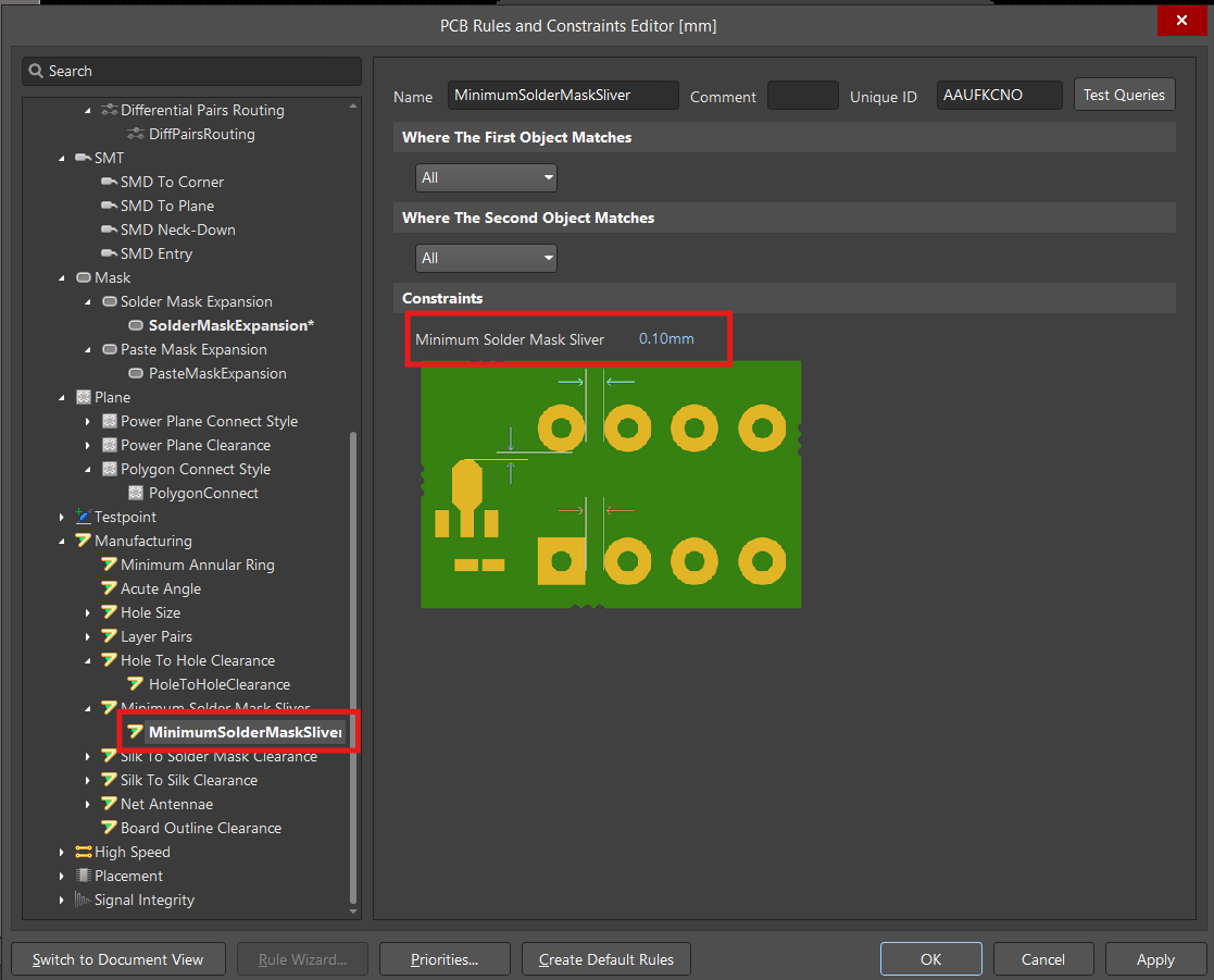
Why 0.1 mm? If you order the standard colors from JLCPCB (Green, Blue, Red, Yellow, Purple), 0.1 mm is their normal capability. Setting it correctly also stops Altium from giving you false DRC errors around fine-pitch ICs.
Note: Black and white solder mask need 0.13 mm. JLCPCB can change these numbers, so check their capabilities page if you're ordering those colors.
2.8 Save the rules
Click Apply to save everything.
Part 3: Layer stackup
Next we set up the layers. We'll need the exact values from JLCPCB's website, and we'll grab them step by step below.
3.1 What is a stackup?
A multi-layer PCB is made of copper layers glued together with insulating material in between. The stackup is the recipe: how many layers, what material each one is, and how thick each one is.
JLCPCB has a few standard stackups. They all end up with the same total board thickness (for example 1.6 mm), but they split that thickness differently between the copper and insulating layers.
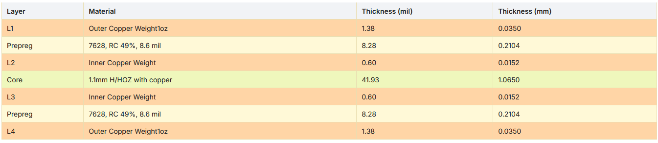
Here's our stackup, from top to bottom (this is the standard JLC04161H-7628):
- Top copper (signals)
- 0.21 mm insulation (prepreg)
- Layer 2 (ground)
- 1.07 mm core
- Layer 3 (power)
- 0.21 mm insulation (prepreg)
- Bottom copper (signals)
3.2 Why does the stackup matter?
Fast signals like USB need controlled impedance so they stay clean. The trace width you need depends on how far the trace is from the ground plane below it:
- Farther from the reference plane → you need a wider trace.
- Closer to the reference plane → you need a narrower trace.
So the stackup decides how wide your traces have to be to hit the impedance you want.
3.3 Why we picked JLC04161H-7628
You can find it here: https://jlcpcb.com/pcb-impedance-calculator/
Note: Scroll to the right on the JLCPCB stackup menu to find this option.
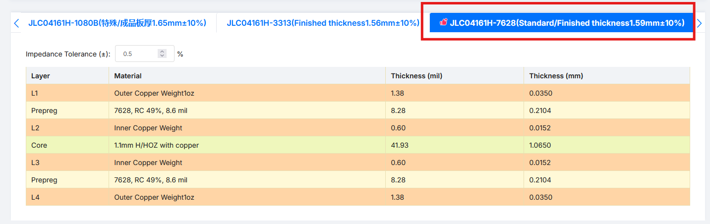
Note: On this stackup the outer layers are 1 oz copper and the inner layers are 0.5 oz.
This is JLCPCB's standard 4-layer stackup. We picked it because:
- It's the default. It's JLCPCB's normal option, so it's well tested and well documented.
- The trace widths are easy to work with. A 50 Ω single-ended trace needs about 0.35 mm (13.8 mil). A 90 Ω differential pair (like USB) needs roughly 0.28 mm per trace with a 0.2 mm gap (we calculate this in Part 4). Both are easy to route on most boards.
- Wider traces handle manufacturing errors better. Small variations affect them less.
- It matches the Phil's Lab tutorial. It uses the same stackup settings.
3.4 When to use a different stackup
You only need another stackup when the standard one can't do what your design needs:
- Thinner dielectrics (1080, 3313, 2116): The reference planes sit closer to the signal layers, so the traces for a given impedance get narrower. Useful for high-density boards, fine-pitch BGA chips, or fast memory like DDR.
- Suffix versions (7628A, 2116B, etc.): These have special layer spacing to fine-tune the differential pair impedance or the insulation between layers.
Rule of thumb: Stick with the standard stackup unless the trace widths for your impedance are too big to fit in your layout.
3.5 Set up the stackup in Altium
Step 1: Open the Layer Stack Manager
While you're in the PCB editor, go to Design > Layer Stack Manager... You'll see the default two-layer setup:
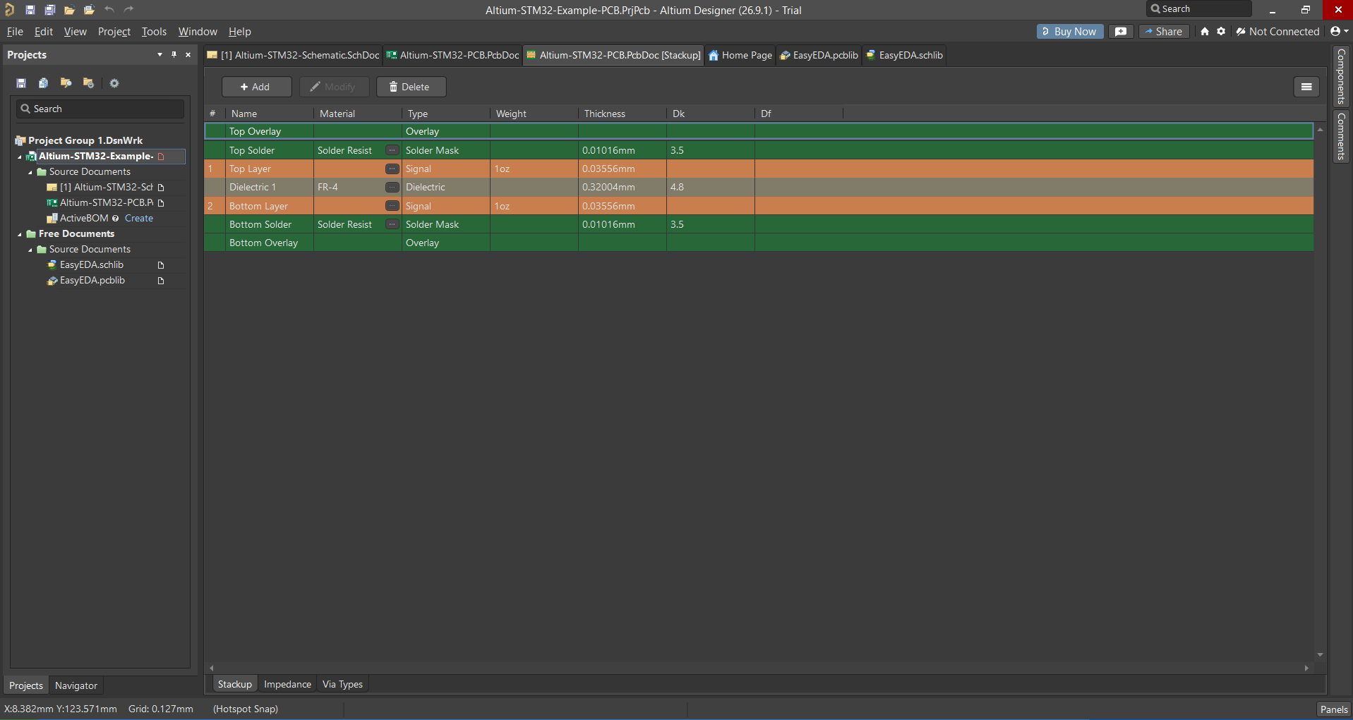
Step 2: Apply the 4-layer preset
In the top menu bar, choose Tools > Presets > 4 Layers. This gives you a basic 4-layer stackup to start from:
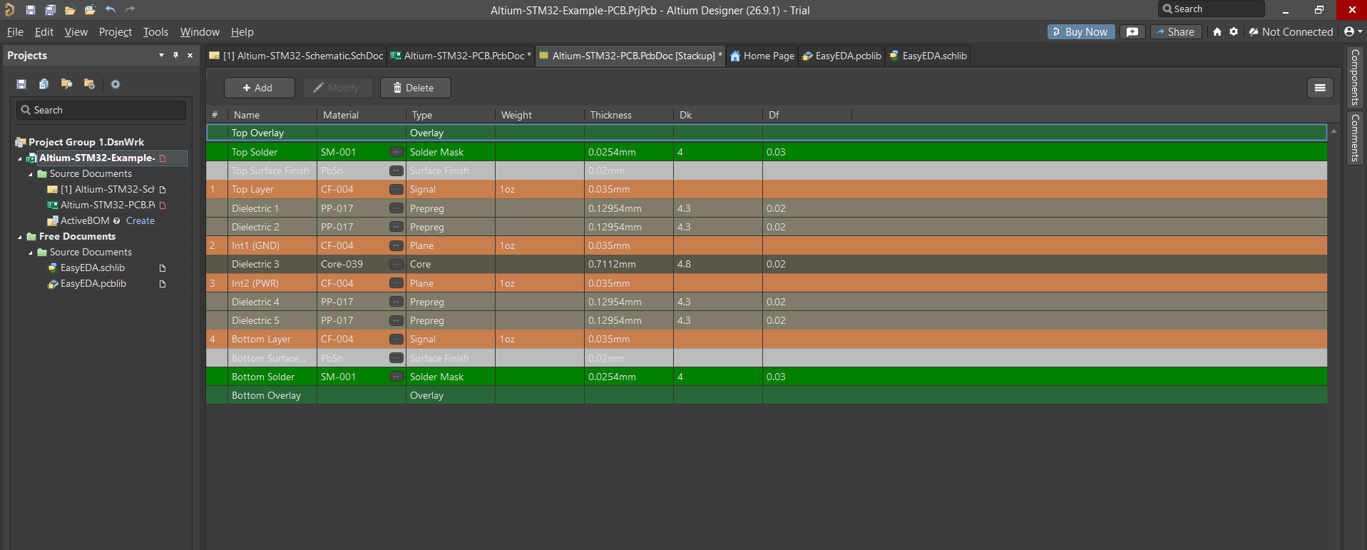
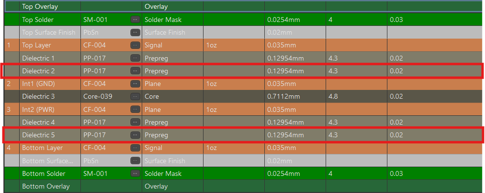
Step 3: Delete the extra prepreg layers
JLCPCB only uses one prepreg layer between a signal layer and a plane layer, but the preset has two. Right-click each extra prepreg layer (the red boxes in the screenshot) and choose Delete. Altium may remove the matching duplicate layer for you when you delete the upper one.
Step 4: Get the thickness values from JLCPCB
Open JLCPCB's impedance page, https://jlcpcb.com/impedance, and look at the JLC04161H-7628 stackup:
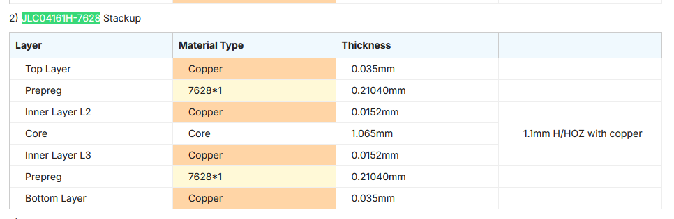
The same table is on the calculator page from section 3.3. It shows the thickness in both mil and mm, so you can copy whichever you need.
Step 5: Type the thicknesses into Altium
Enter those values in the Layer Stack Manager:
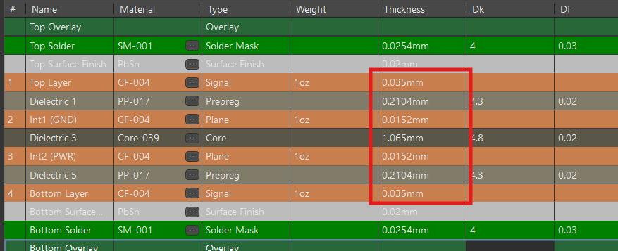
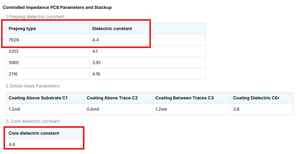
Step 6: Get the dielectric constants (Dk)
The Dk tells Altium how the insulating material affects the signals. Get the Dk for the core and the prepreg from JLCPCB: https://jlcpcb.com/impedance
For our stackup that's 4.4 for the 7628 prepreg and 4.6 for the core.
Step 7: Type the Dk values into Altium
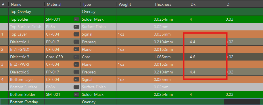
This makes Altium's impedance calculations match what JLCPCB will actually build.
Step 8: Change the inner copper to 0.5 oz
Change the copper weight of the inner layers (Int1 and Int2) from 1 oz to 1/2 oz. This matches JLCPCB's standard inner layers.
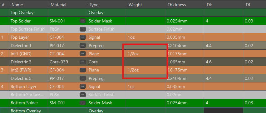
Heads up: In our screenshot, Altium changed the inner copper thickness to 0.0175 mm when we switched to 1/2 oz. JLCPCB's value is 0.0152 mm, so after you change the weight, type 0.0152 mm back in.
Notes on Dk and Df:
- The Material column fills in default Dk and Df values. When you type in the Dk from JLCPCB, it replaces the default.
- Df (dissipation factor) for normal FR-4 below 1 GHz usually doesn't matter much for a design like this, so we don't touch it.
- Dk changes a little at higher frequencies, but JLCPCB's fixed values are good enough for the frequencies we're working with.
Step 9: Set the inner layers to Signal
Change the type of the inner layers from Plane to Signal. We'll add our ground and power planes later as copper pours.
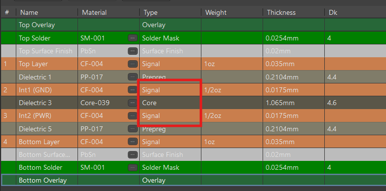
Why? If you leave them as Plane, Altium exports them as negative layers in the Gerber files. That works, but it's easy to get wrong and it's not ideal. Using Signal layers with polygon pours avoids the problem.
Part 4: Impedance and trace widths
Altium has its own impedance calculator. Before using it, it helps to know how these calculations work, so you know how much to trust the numbers.
4.1 Ways to calculate impedance
Source: https://www.youtube.com/watch?v=raG6piNjtxE&t=445s
What this means in simple terms:
- Most web calculators use IPC-2141 or Wadell's equations. Both are formulas that give you a good estimate, not an exact answer.
- IPC-2141 is the quickest but the least precise.
- Wadell's equations work over a wider range of impedances, but they're still approximations.
- Field solvers (2D and 3D) work out the actual electric fields, so they're much more accurate. The 3D one is the most accurate, but it's also the hardest to use and the slowest.
- KiCad doesn't have a built-in 2D or 3D field solver, so you'd need an external open-source tool for that.
- Altium's built-in calculator uses a 2D field solver, so it's a good choice.
Note: If you use a formula-based calculator, take a look at what assumptions its equations make before you trust the result.
4.2 Use Altium's impedance calculator
- Open the Layer Stack Manager and click the Impedance tab at the bottom.
- Set the trace gap to 8 mil. Altium converts it to mm for you (0.2032 mm).
- In the Properties panel, set Type to Differential and Target Impedance to 90 (Ω).
- Altium calculates the trace width for you.
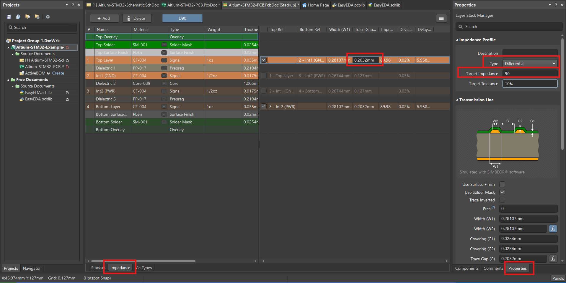
In our screenshot, Altium gives a trace width of about 0.281 mm for a 90 Ω pair (it shows 89.98 Ω), with a 0.2032 mm gap.
Tip: Use this width in a separate rule for your USB (or other 90 Ω) pairs, with a higher priority than the general Width rule from section 2.3. If you don't, Altium will use the general rule for those traces.
Quick cheat sheet
Project settings
Design rules
Stackup (JLC04161H-7628)
Impedance